0.18-micron, 6-layer metal CMOS
125-MHz operation
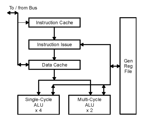
8-kbyte data cache
8-kbyte instruction cache
64-bit asynchronous bus
vector processing facility
4 integer or logical operations per cycle
4 logarithmic multiplies, divides or square-roots / cycle
2 logarithmic adds or subtracts / 3 cycles
single-level interrupt
1.8-V core; 3.3-V I/O
development and evaluation system for PC-based host
relocating assembler
linkage editor
mathematical function library
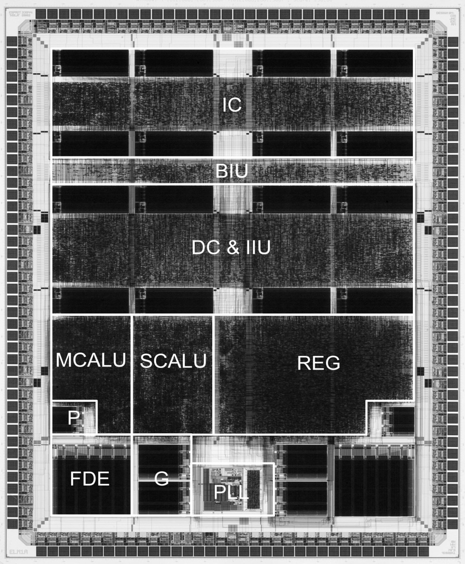
Legend
IC: instruction cache
DC: data cache
IIU: instruction issue unit
BIU: bus interface unit
SCALU: single cycle ALUs
MCALU: multi cycle ALUs
REG: general registers
F,D,E and P: interpolator lookup tables (mirrored for two MCALUs)
G: transform tables (mirrored)
PLL: phase-locked loop